Groundbreaking crystal oxide transistors are faster, smaller and more reliable than silicon
New crystal oxide transistor outperforms silicon, offering faster, smaller, and more reliable tech for AI and data-driven devices.
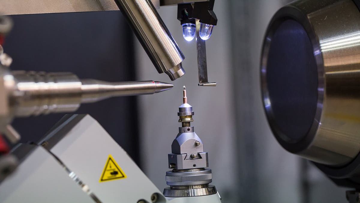
New crystal-based transistor could replace silicon in next-gen electronics. (CREDIT: CC BY-SA 4.0)
Shrinking computers, faster phones, and smarter gadgets all rely on one tiny component: the transistor. Invented in the 20th century, it’s what powers nearly every modern electronic device. Transistors act like switches, turning electrical signals on or off or boosting them when needed.
But as tech companies push to make devices smaller and more powerful, there’s growing concern that traditional silicon-based transistors may have reached their limits. Making them any smaller is becoming extremely difficult.
The Limitations of Silicon
For decades, engineers have been shrinking silicon transistors to pack more onto microchips. This has allowed smartphones to get thinner, laptops to get lighter, and cloud computing to become faster. But as silicon gets scaled down further, issues like overheating, power leakage, and instability become harder to manage. The atomic structure of silicon just doesn’t perform well when pushed to such small sizes.
In the race to solve this, a team from the Institute of Industrial Science at The University of Tokyo may have found a better way forward. Rather than working around silicon’s limits, they chose to bypass it entirely.
Building a New Kind of Transistor
In their study—soon to be presented at the 2025 Symposium on VLSI Technology and Circuits—the researchers introduced a brand-new transistor built from gallium-doped indium oxide. This material, known as InGaOx, belongs to a class called crystalline oxides. Unlike silicon, it forms a neatly ordered crystal lattice that allows electrons to move more freely, which is essential for fast and efficient electronic devices.
“We also wanted our crystalline oxide transistor to feature a ‘gate-all-around’ structure, whereby the gate, which turns the current on or off, surrounds the channel where the current flows,” said lead author Anlan Chen. This type of structure offers much better control than traditional transistors, where the gate only sits on one side. Wrapping the gate entirely around the channel means fewer errors and more consistent performance, even at very small sizes.
Related Stories
To make this happen, the team had to adjust the properties of indium oxide. They did this by doping it with gallium. This process involves adding small amounts of another element to improve the material’s performance.
“Indium oxide contains oxygen-vacancy defects, which facilitate carrier scattering and thus lower device stability,” explained senior author Masaharu Kobayashi. “We doped indium oxide with gallium to suppress oxygen vacancies and in turn improve transistor reliability.”
A Precision Process With Atomic-Level Control
Constructing this transistor wasn’t easy. The researchers used a technique called atomic-layer deposition. This method lays down one atomic layer at a time, allowing for extreme precision. Each layer of InGaOx was deposited carefully onto the channel region of the transistor. After layering, they applied heat to turn the material into its crystalline form, which is essential for high electron mobility.
This new transistor—technically a metal oxide-based field-effect transistor, or MOSFET—features the gate-all-around design wrapped around a gallium-doped oxide channel. The result is a compact and powerful device with excellent electrical performance.
“Our gate-all-around MOSFET, containing a gallium-doped indium oxide layer, achieves high mobility of 44.5 cm² per volt-second,” said Dr. Chen. “Crucially, the device demonstrates promising reliability by operating stably under applied stress for nearly three hours. In fact, our MOSFET outperformed similar devices that have previously been reported.”
That number—44.5 cm²/Vs—is a key indicator of how easily electrons can flow through the material. A higher value means faster response times and lower energy loss, which are crucial for next-gen electronics.
Toward the Future of Smart Tech
While this transistor might be tiny, its impact could be enormous. The combination of high mobility and stable performance makes it a strong candidate for future tech that demands heavy computing power. That includes systems behind artificial intelligence, massive data centers, and advanced wearable tech.
This isn’t just about making phones or computers faster. It’s about enabling entire industries to build smarter machines that can learn, adapt, and make decisions. That requires processing vast amounts of information quickly, and today’s silicon-based transistors can no longer keep up on their own.
The new design also opens the door to even more miniaturized electronics. As devices shrink, packing more power into smaller spaces becomes essential. Gallium-doped indium oxide, with its crystal-like structure and high electron mobility, could lead the way.
A Big Leap for Small Tech
This development from Tokyo is more than just a clever engineering trick. It represents a shift in how we think about materials in electronics. By reimagining both what a transistor is made of and how it is built, researchers are unlocking new levels of performance. The move away from silicon marks a key moment in the history of microelectronics.
It’s also a reminder that innovation often happens when we stop trying to stretch old tools and instead reach for something entirely new. With the help of atomic-layer precision and material science, this new transistor may help shape the future of computing, communication, and smart devices.
Whether powering next-gen artificial intelligence or driving advances in wearable health tech, these transistors offer a foundation for more reliable and efficient electronics. As the world becomes increasingly connected, developments like these will play a key role in making technology not only faster and smaller but also smarter and more sustainable.
Note: The article above provided above by The Brighter Side of News.
Like these kind of feel good stories? Get The Brighter Side of News' newsletter.