Light-based computer breakthrough: Scientists create the world’s first 2D photonic circuits
In the age of connectivity where data travels at the speed of light, guiding and transporting that light is pivotal.
[Aug. 14, 2023: Staff Writer, The Brighter Side of News]
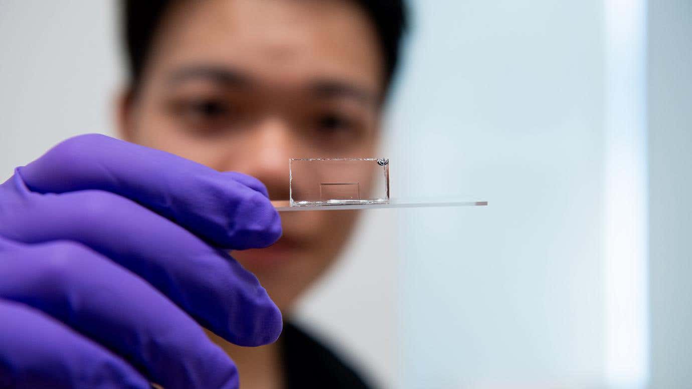
Scientists at the University of Chicago found a glass crystal just a few atoms thick can trap and carry light—and could be used for applications. The material is visible as the thin line in the center of the plastic, held by study co-author Hanyu Hong. (CREDIT: Photo by Jean Lachat)
In the age of connectivity where data travels at the speed of light, guiding and transporting that light is pivotal. This light – an intricate tapestry of YouTube videos, financial transactions, and digital interactions – crisscrosses the world through hair-sized strands known as fiber optic cables.
However, a pioneering research team led by University of Chicago's Prof. Jiwoong Park has posed an intriguing question: What if these light-carrying strands were not just thinner but essentially two-dimensional? The results of this curiosity, published on in the renowned journal Science, promise to usher in a new era of technology, making strides into the domain of 2D photonic circuits.
At the heart of this breakthrough is a super-thin sheet of glass crystal, so thin it boasts just a few atoms in thickness. Yet, it holds a potential so grand that it could redefine our understanding of light-based computing.
Through meticulous experiments, Prof. Park and his team discovered that this 2D glass crystal can not only confine light but also transmit it efficiently over distances up to a centimeter. Given the nano-scale realm of photonic circuits, this is a staggering achievement.
Related Stories
"We were utterly surprised by how powerful this super-thin crystal is; not only can it hold energy, but deliver it a thousand times further than anyone has seen in similar systems,” remarked Prof. Jiwoong Park, who apart from spearheading the study, also holds prestigious positions at the James Franck Institute and Pritzker School of Molecular Engineering. He further added, "The trapped light also behaved like it is traveling in a 2D space.”
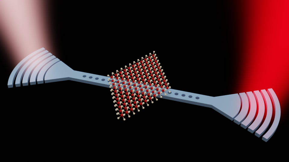
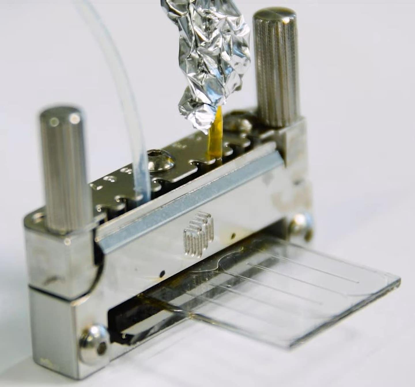
This newly introduced system, in essence, is a two-dimensional waveguide for directing light. During their experimental runs, the team used minuscule prisms, lenses, and switches, directing the light's path along a chip – foundational components for constructing circuits and computation processes.
While three-dimensional photonic circuits are not new, the Park team's 2D innovation differs significantly. Conventional waveguides completely encase the traveling light particles, known as photons. But in the novel 2D system, since the glass crystal's thickness is less than that of a photon, part of the photon protrudes as it navigates through.
Prof. Jiwoong Park (at left) and scientist Hanyu Hong (at right) examine the material in Park’s lab at the University of Chicago. In tests, they could use tiny prisms, lenses, and switches to guide the path of the light along a chip—all the ingredients for circuits and computations. (CREDIT: Photo by Jean Lachat)
To draw a real-world parallel, imagine comparing an airport's suitcase tube system with a conveyor belt. Suitcases on the conveyor belt, exposed to the external environment, are more accessible, allowing easy adjustments during their journey. Similarly, the exposed nature of photons in the 2D crystal system permits the crafting of sophisticated devices and offers potential applications like environment-sensitive sensors.
“For example, say you had a sample of liquid, and you wanted to sense whether a particular molecule was present,” elucidated Park. “You could design it so that this waveguide travels through the sample, and the presence of that molecule would change how the light behaves.”
Prof. Jiwoong Park (at left) and scientist Hanyu Hong (at right) in the laser lab, where they confirmed the material could carry light – even though it’s smaller than the light itself. (CREDIT: Photo by Jean Lachat)
While molybdenum disulfide was the material of choice in these trials, the underlying principles could be adapted for other substances, expanding potential applications and innovations.
Though theoretical models had long hinted at such behaviors, turning theory into practice required perseverance. "It was a really challenging but satisfying problem, because we were walking into a completely new field. So everything we needed we had to devise ourselves—from growing the material to measuring how the light was moving,” expressed Hanyu Hong, a graduate student and the co-first author of the paper.
Research demonstrates what are essentially 2D photonic circuits, and could open paths to new technology. (CREDIT: Science)
Contributions to this groundbreaking paper also came from Myungjae Lee (formerly a postdoc at UChicago, now a faculty member at Seoul National University) and postdoctoral researcher Jaehyung Yu, with Fauzia Mujid (PhD’22, now at Ecolab) and graduate students Andrew Ye and Ce Liang.
The dedicated facilities at the University of Chicago Materials Research Science and Engineering Center, the Pritzker Nanofabrication Facility, and the Cornell Center for Materials Research were instrumental in turning this vision into reality.
As the world stands at the cusp of technological evolution, endeavors like Prof. Park's shed light on a future where boundaries are continually pushed, and the unimaginable becomes the norm. The evolution from 3D to 2D photonic circuits, though nascent, holds the promise of rewriting technological narratives, with exciting times ahead for the world of light-based computing.
Note: Materials provided above by The Brighter Side of News. Content may be edited for style and length.
Like these kind of feel good stories? Get the Brighter Side of News' newsletter.