New 3D-printable material paves the way for cheaper and sustainable OLED televisions and smartphones
Researcher has introduced “supramolecular ink,” a revolutionary technology poised to transform OLED (organic light-emitting diode) displays

[Jan. 23, 2024: JD Shavit, The Brighter Side of News]
Unlike their predecessors that relied on costly and scarce metals, this innovative ink utilizes inexpensive, Earth-abundant elements. (CREDIT: Creative Commons)
In a groundbreaking development, a research team led by Lawrence Berkeley National Laboratory (Berkeley Lab) has introduced "supramolecular ink," a revolutionary technology poised to transform OLED (organic light-emitting diode) displays and electronic devices.
Unlike their predecessors that relied on costly and scarce metals, this innovative ink utilizes inexpensive, Earth-abundant elements, offering the promise of more affordable and environmentally sustainable flat-panel screens and electronic gadgets.
Principal investigator Peidong Yang, a faculty senior scientist in Berkeley Lab's Materials Sciences Division and a professor of chemistry and materials science and engineering at UC Berkeley, emphasized the transformative potential of this breakthrough: "By replacing precious metals with Earth-abundant materials, our supramolecular ink technology could be a game changer for the OLED display industry."
He further noted, "What's even more exciting is that the technology could also extend its reach to organic printable films for the fabrication of wearable devices as well as luminescent art and sculpture."
Related Stories
The significance of this innovation becomes apparent when considering the ubiquity of OLED screens in modern devices, including smartphones and flat panel TVs. OLEDs have gained widespread adoption due to their lightweight, slim profile, energy efficiency, and superior picture quality.
Unlike traditional LCD displays, OLEDs emit light directly from tiny organic molecules, eliminating the need for a backlight layer. However, the inclusion of rare and expensive metals like iridium has posed sustainability and cost challenges.
The Berkeley Lab research team recently detailed their revolutionary material in a study published in the journal Science, unveiling a solution to these pressing issues. The supramolecular ink is composed of hafnium (Hf) and zirconium (Zr) powders, which can be mixed at low temperatures, ranging from room temperature up to approximately 176 degrees Fahrenheit (80 degrees Celsius), to form a semiconductor "ink."
Crystal structure of (18C6@K)2ZrBr6 determined by single crystal x-ray diffraction. (A) The unit cell viewed along the c axis direction. (B) The unit cell viewed along the direction perpendicular to the c axis. (CREDIT: journal Science)
A key aspect of this technology is the self-assembly of tiny molecular "building block" structures within the ink, a process referred to as supramolecular assembly. Cheng Zhu, co-first author of the paper and a Ph.D. candidate in materials science and engineering at UC Berkeley, drew an intriguing analogy: "Our approach can be compared to building with LEGO blocks." This supramolecular assembly enables stable and high-purity synthesis at low temperatures, making it a game-changing method in semiconductor manufacturing.
Spectroscopy experiments conducted at UC Berkeley demonstrated that the supramolecular ink composites are highly efficient emitters of blue and green light, essential attributes for energy-efficient OLED emitters in electronic displays and 3D printing. Optical experiments further revealed that these compounds exhibit near-unity quantum efficiency, an exceptional ability to convert nearly all absorbed light into visible light during the emission process.
To showcase the material's versatility, the researchers fabricated a thin-film display prototype from the composite ink. The results were promising, with the material proving suitable for programmable electronic displays. Zhu highlighted one of their achievements, stating, "The alphabet movie serves as a compelling example that illustrates the application of emissive thin films like supramolecular ink in the creation of fast-switching displays."
Further experimentation at UC Berkeley confirmed that the supramolecular ink is compatible with 3D printing technologies, offering exciting prospects for decorative OLED lighting designs. Zhu suggested that manufacturers could leverage this ink to create wearable devices or high-tech clothing designed for safety in low-light conditions, or even wearable devices that display information through supramolecular light-emitting structures.
Eiffel Tower-shaped luminescent structures 3D-printed from supramolecular ink. Each 2-centimeter-tall device is fabricated from supramolecular ink that emits blue or green light when exposed to 254-nanometer ultraviolet light. (CREDIT: Peidong Yang and Cheng Zhu/Berkeley Lab. Courtesy of Science)
This development represents yet another testament to the Peidong Yang lab's commitment to sustainable materials for cost-effective and energy-efficient semiconductor manufacturing. In the previous year, Yang and his team introduced a "multielement ink," the first "high-entropy" semiconductor that can be processed at low or room temperature.
Moreover, the demonstrated stability and shelf life of the supramolecular ink compounds open doors to the commercial advancement of ionic halide perovskites, a thin-film solar material that has long captured the display industry's interest.
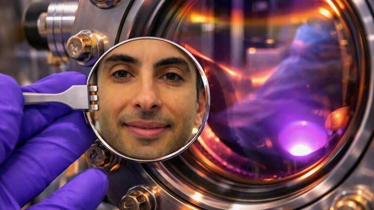
A new 3D-printable material called “supramolecular ink” replaces costly scarce metals with inexpensive, Earth-abundant materials. (CREDIT: Jenny Nuss/Berkeley Lab. Courtesy of Science)
These perovskites, while offering potential cost benefits, typically contain lead, a concern for environmental and public health. In stark contrast, the new supramolecular ink, belonging to the ionic halide perovskite family, offers a lead-free formulation without sacrificing performance.
Looking ahead, the researchers are embarking on an exploration of the material's electroluminescent potential. Zhu explained, "This involves a focused and specialized investigation into how well our materials can emit light using electrical excitation. This step is essential to understanding our material's full potential for creating efficient light-emitting devices."
With its potential to revolutionize OLED displays, 3D printing, wearable tech, and more, this innovation holds the promise of a brighter, more energy-efficient future in the world of electronics.
Note: Materials provided above by The Brighter Side of News. Content may be edited for style and length.
Like these kind of feel good stories? Get the Brighter Side of News' newsletter.