New photonic chip enables exponentially faster and more energy-efficient artificial intelligence
Researchers have developed an innovative and energy-efficient method for transferring larger amounts of data over fiber-optic cables.
[July 9, 2023: Staff Writer, The Brighter Side of News]
Researchers have developed an innovative and energy-efficient method for transferring larger amounts of data over fiber-optic cables. (CREDIT: The Lightwave Research Laboratory/Columbia Engineering)
The current landscape of high-performance computers and data centers, often utilized to run advanced artificial intelligence programs such as large language models, is not constrained by the computing capacity of their individual nodes. In fact, a more pressing concern, the so-called "bandwidth bottleneck," is the major factor impeding performance enhancement and scaling of these systems.
The principal challenge lies in the amount of data these systems can shuttle between the nodes, a factor primarily defined by the method and efficiency of data transfer.
The nodes within these systems, which can be dispersed over distances greater than a kilometer, must find a way to transmit data rapidly and efficiently. Typically, metal wires fall short due to their tendency to dissipate electrical signals as heat at high speeds. Therefore, data transfer in these settings usually relies on fiber-optic cables, albeit with a significant energy penalty in the conversion of electrical data into optical data, and vice versa.
However, a groundbreaking study published today in the prestigious Nature Photonics journal offers a new perspective. Columbia Engineering researchers have developed an innovative and energy-efficient method for transferring larger amounts of data over fiber-optic cables connecting the nodes.
Related Stories
This pioneering technology promises to redefine the existing techniques of transmitting multiple signals concurrently over the same fiber-optic cables.
In the conventional approach, each wavelength of light requires a separate laser to generate it. In stark contrast, the novel chips developed by the Columbia team need only a single laser to spawn hundreds of unique light wavelengths. Each wavelength can independently transfer streams of data, facilitating a marked boost in data transfer volume.
A breakthrough in energy-efficient data transfer
The researchers adopted a technique known as wavelength-division multiplexing (WDM) and utilized devices called Kerr frequency combs to achieve this feat. A Kerr frequency comb receives a single color of light and emits multiple new colors, thereby creating a broad spectrum of light. These tools were pivotal in the process, enabling the researchers to transmit clear signals via separate and distinct light wavelengths, each with space between them.
Illustration of a disaggregated data center based on Kerr frequency comb-driven silicon photonic links. (CREDIT: Lightwave Research Laboratory/Columbia Engineering)
The research team, under the guidance of Michal Lipson, Higgins Professor of Electrical Engineering and Professor of Applied Physics, and Alexander Gaeta, David M. Rickey Professor of Applied Physics and Materials Science and Professor of Electrical Engineering, saw potential in these devices for optical communication. They envisaged encoding independent information channels on each color of light and transmitting them over a single optical fiber.
Keren Bergman, the senior author of the study and Charles Batchelor Professor of Electrical Engineering at Columbia Engineering, states, “We recognized that these devices make ideal sources for optical communications." Bergman, who also heads the Columbia Nano Initiative, anticipates the implications of this technological leap in data transfer – the potential to transmit exponentially more data without proportionately increasing energy consumption.
Photonic Integrated Chip placed on a dime. (CREDIT: Lightwave Research Laboratory/Columbia Engineering)
The team successfully miniaturized the optical components, incorporating them onto chips that measured only a few millimeters on each edge. These chips generate light, encode it with electrical data, and then convert the optical data back into an electrical signal at the target node.
To maintain the clarity and precision of the data, the team conceived an innovative photonic circuit architecture, allowing each channel to be individually encoded with minimal interference from neighboring channels. This clever design means the signals transmitted in each color of light remain distinct, easing their interpretation and conversion back into electronic data by the receiver.
The compact and efficient approach to revolutionizing data centers
Anthony Rizzo, the lead author of the study, conducted this groundbreaking work during his PhD tenure in Bergman's lab and is currently a research scientist at the U.S. Air Force Research Laboratory Information Directorate. He pointed out the compactness and energy-efficiency of their approach, emphasizing, "In this way, our approach is much more compact and energy-efficient than comparable approaches." The silicon nitride comb generation chips employed in the system can be manufactured in standard CMOS foundries used to produce microelectronics chips, rather than in the more costly dedicated III-V foundries. This characteristic not only reduces costs but also eases the scaling process.
This compact design has another significant advantage - it enables the chips to directly interface with computer electronics chips. This direct link greatly reduces total energy consumption as the electrical data signals only have to traverse millimeters of distance rather than tens of centimeters.
Bergman noted, "What this work shows is a viable path towards both dramatically reducing the system energy consumption while simultaneously increasing the computing power by orders of magnitude." This breakthrough, she added, would allow AI applications to continue expanding exponentially, but with minimal environmental impact.
Promising results point to real-world deployment
In their experimental setup, the researchers achieved remarkable results. They transmitted 16 gigabits per second per wavelength across 32 distinct wavelengths of light, amassing a total single-fiber bandwidth of 512 Gb/s. Furthermore, they recorded an incredibly low error rate—less than one bit in one trillion transmitted bits of data. These high levels of speed and efficiency were achieved using silicon chips with dimensions of 4 mm x 1 mm (transmitter) and 3 mm x 1 mm (receiver), each smaller than a human fingernail.
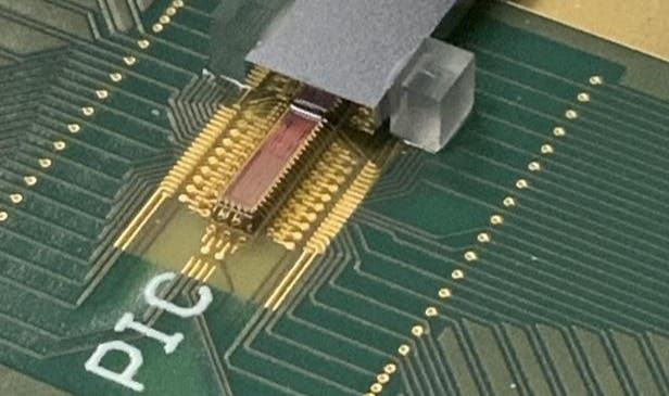
Photonic integrated link driven by Kerr frequency comb. (CREDIT: The Lightwave Research Laboratory/Columbia Engineering)
"While we used 32 wavelength channels in the proof-of-principle demonstration, our architecture can be scaled to accommodate over 100 channels, which is well within the reach of standard Kerr comb designs," Rizzo stated. Moreover, these chips can be fabricated using the same facilities that manufacture the microelectronics chips found in everyday consumer electronics, further simplifying the path towards real-world deployment.
As the team looks to the future, they aim to merge the photonics with chip-scale driving and control electronics, further miniaturizing the system. If successful, this technology could redefine the landscape of high-performance computers and data centers, facilitating a new era of efficient and powerful artificial intelligence applications.
For more science and technology news stories check out our New Innovations section at The Brighter Side of News.
Note: Materials provided above by The Brighter Side of News. Content may be edited for style and length.
Like these kind of feel good stories? Get the Brighter Side of News' newsletter.