Physicists explain the remarkable energy-harvesting efficiency of perovskite solar cells
Perovskites thrive on imperfections. Domain wall networks may split charges and guide them like internal highways, even with no voltage.

 Edited By: Joshua Shavit
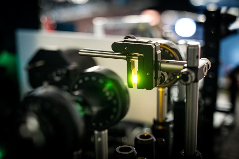
Examining a lead-halide perovskite crystal in the lab using optical methods. The sample (center right) glows green. (CREDIT: ISTA)
Light can hit a lead halide perovskite crystal that is anything but pristine and still end up as useful electric current. That mismatch has bothered solar researchers for more than a decade. Silicon needs an almost spotless lattice. Perovskites, grown cheaply from solution, are packed with defects, strain, and disorder. Yet their solar-cell efficiencies have climbed into the same neighborhood.
A new paper in Nature Communications from physicists at the Institute of Science and Technology Austria (ISTA) argues that the mess is not a side issue. It is the mechanism.
Postdoc Dmytro Rak and assistant professor Zhanybek Alpichshev report that perovskites such as MAPbBr3 host dense networks of microscopic domain walls, boundaries between small regions of slightly different strain. Those walls, they say, carry localized flexoelectric polarization that creates internal electric fields. The fields can split newly created electron hole pairs and keep them apart long enough to move. In perovskites, the “defects” can become the route, not the roadblock.
A material that should not behave this way
Solar cells do two things well or they fail: they absorb light, and they keep the resulting charges from recombining before the electrodes collect them. When a photon excites the material, it can produce a negatively charged electron and a positively charged hole. The hard part is making them travel far enough to be extracted. In silicon, the classic answer is purity. Remove traps. Reduce defects. Give charges a clean lane.
Solution processed lead halide perovskites do not look like that kind of system. They are often discussed as “defect tolerant,” yet a basic puzzle remains. Evidence suggests that when electrons and holes form a bound exciton in these materials, it can recombine quickly. At the same time, measurements show electrons and holes can remain separated for surprisingly long times, enabling long diffusion lengths and strong photovoltaic performance.
Rak and Alpichshev frame the contradiction as a sign that something inside the crystal is doing active work: forces strong enough to pull opposite charges apart, even without an applied voltage.
The first clue was optical, and it was awkward
The study focuses on the room temperature polymorph of MAPbBr3. It is commonly identified as cubic above about 230 K, a symmetry that should be optically isotropic. A truly cubic crystal should not show birefringence.
But the team observed unexpected optical anisotropy. In a crossed polarizer setup with a 632.8 nm He Ne laser beam incident normal to the (001) plane, the crystal showed a complex birefringent pattern. That matters because birefringence in a nominally cubic system points to strain, and strain that varies in space points to defects or domain boundaries.
The temperature dependence of the cumulative phase retardation across the cubic to tetragonal transition kept the sharp anomaly at the nominal transition, while the high temperature birefringence looked like a simple offset. The authors interpret that as a sign that the room temperature symmetry lowering has a different origin than the low temperature octahedral rotations that drive the tetragonal phase.
In plain terms, something structural is happening in the “cubic” phase that does not fit the neat picture.
Silver ions as a kind of angiography
Seeing internal structure deep in a crystal is hard. Surface probes can miss what happens in the bulk. The ISTA team took an unusual approach: stain the internal defect network from the inside out.
They injected silver ions electrophoretically into MAPbBr3 under an applied electric field. The idea is that ions diffuse into the bulk and preferentially cluster near defect sites. Then the ions are reduced to metallic silver, producing visible patterns under a microscope. The authors compare it to angiography, except the “vessels” are the crystal’s defect boundaries.
The resulting images showed dendritic patterns aligned at 45 and 90 degrees relative to the crystal axes, consistent with 90 degree and 180 degree domain walls. They report domains as small as about 5 by 5 microns squared. Focus stacked images and a Z stack showed the structure runs through the bulk, not just the surface.
One potential concern is whether the electric field used for staining could create or rearrange the domain walls, especially in a material known for ion migration. The team ran time dependent staining steps and found that domain walls visible at the onset remained unchanged under repeated application of the field, which they take as evidence that the staining reveals a pre existing pattern rather than writing a new one. They also observed that the silver features fade after the field is removed, with near complete dissolution over days.
A current with no voltage
Strain gradients can break inversion symmetry locally and generate polarization through flexoelectricity. The authors propose that in MAPbBr3, these gradients are concentrated at domain walls. That could create local electric fields capable of separating charges.
To test for internal fields, they injected carriers deep inside the crystal using sub bandgap ultrafast laser pulses that generate electron hole pairs through two photon absorption. They then measured photocurrent using two pairs of carbon leads attached to the sample’s sides, mapping current as they scanned the excitation spot.
They observed a finite zero bias photocurrent after localized injection. The current depended strongly on where in the sample carriers were created, and the sign remained constant across large regions that were not symmetric about the sample midplane.
The authors argue that this is inconsistent with a dynamic flexoelectric effect and is better explained by an electrostatic potential landscape tied to a network of flexoelectrically polarized domain walls. In their schematic, potential is flat within domains and changes abruptly at walls, so the average slope can set the current sign.
They also connect this to a long running argument about “ferroelectricity” in lead halide perovskites. If polarization is confined to domain walls, it can produce pyroelectric like signals and hysteresis under external fields, while leaving bulk inversion symmetry intact. They note that this aligns with reports where second harmonic generation supports centrosymmetry in the bulk.
The paper also reports similar zero bias two photon photocurrent in bulk MAPbI3, and suggests localized flexoelectricity could be present in both tetragonal and cubic phases. They point to the observation that MAPbI3 device efficiency reportedly remains largely unaffected by the tetragonal to cubic transition as a clue that the underlying mechanism persists across phases.
Why the current can last without net charge transfer
A zero bias current in an insulating sample raises an immediate issue. If electrons drift one way and holes the other indefinitely, you would expect charge buildup that shuts the process down. Yet the authors observed photocurrent generation for hours without major change in magnitude.
They address this by arguing the observed current is a displacement current tied to changes in polarization, not sustained net charge transfer. They note that their digital lock in amplifier has bandwidth limits that can miss fast features, so a measured transient can look inconsistent with the requirement that polarization returns to its initial state after each pulse. To test the “no net transfer” claim, they measured the average photocurrent with a high sensitivity analog electrometer over long integration times and report that on average there is no net charge transfer.
Then they zoom in on the transient shape. They describe two regimes after a laser pulse: a fast polarization buildup over a few microseconds associated with a narrow spike, and a slower relaxation around 100 microseconds that forms a long tail with opposite sign. Their microscopic picture is that carriers diffuse to domain boundaries where local fields split them, trapping electrons and holes on opposite sides of the wall. Recombination then requires tunneling through a flexoelectric potential barrier.
That tunneling barrier is the heart of the “long life in a defective material” idea. If electrons and holes sit on opposite sides of a wall, recombination slows dramatically. The authors argue this can reconcile nanosecond scale exciton lifetimes with much longer photocurrent relaxation times.
Not a neat exponential, and that matters
A simple exponential decay would suggest a fixed recombination rate. The team reports that the regime II current tail is better described by a different time dependence than single or bi exponential decay. They present an unusual correlation between current magnitude and decay rate when fitting parts of the transient with an exponential, which they say emerges naturally from their proposed decay form.
They connect this to density dependent tunneling. As charge accumulates at a domain wall, they propose it reduces the effective band gap locally and increases tunneling probability exponentially. That would make the recombination rate depend on carrier density. It also offers a reason for extreme sensitivity to weak ambient light, which they show can modify photocurrent transients.
Domain walls as charge highways
Once the domain wall network is real, the energy story becomes simpler. Charges do not need to survive in the bulk for long. They need to get to a wall, separate, and then move along it.
In the authors’ picture, a domain wall provides both separation and transport. The local electric field pulls electrons and holes to opposite sides of the wall. That spatial separation suppresses recombination. Meanwhile, carriers can move along the wall over long distances, effectively turning these boundaries into mesoscale conductive pathways.
The paper compares the idea to conductive domain walls in ferroelectric BaTiO3 and to earlier proposals of “ferroelectric highways” in lead halide perovskites, but grounds it in a flexoelectric domain wall mechanism in nominally cubic MAPbBr3.
There is also a caution built into their discussion. If too much charge piles up at domain walls under high illumination, the same charging can boost tunneling rates and accelerate recombination. So domain walls might both help and, in some conditions, limit performance. The authors call for systematic work that combines experimental characterization and modeling to understand that balance in real devices.
Research findings are available online in the journal Nature Communications.
The original story "Physicists explain the remarkable energy-harvesting efficiency of perovskite solar cells" is published in The Brighter Side of News.
Related Stories
- Thin, new design doubles the efficiency of OLED lights
- Solar energy is now the world’s cheapest and fastest-growing energy source
- Scientists create indoor solar cells that could eliminate billions of batteries
Like these kind of feel good stories? Get The Brighter Side of News' newsletter.
Rebecca Shavit
Writer
Based in Los Angeles, Rebecca Shavit is a dedicated science and technology journalist who writes for The Brighter Side of News, an online publication committed to highlighting positive and transformative stories from around the world. Her reporting spans a wide range of topics, from cutting-edge medical breakthroughs to historical discoveries and innovations. With a keen ability to translate complex concepts into engaging and accessible stories, she makes science and innovation relatable to a broad audience.