Scientists shrink a lab-grade spectrometer down to the size of a grain of sand
Researchers at UC Davis have developed a spectrometer-on-a-chip that replaces bulky optics with silicon detectors and artificial intelligence.
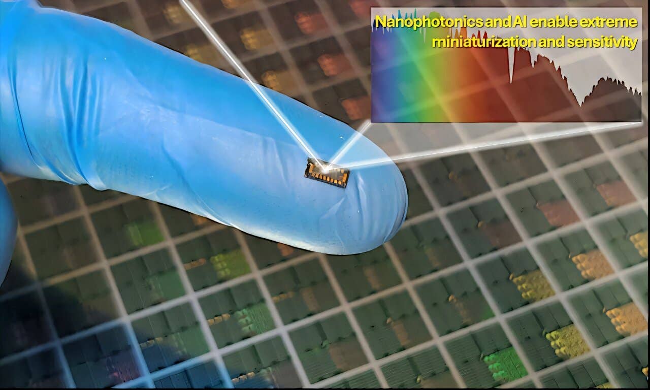
Resting on a fingertip, this miniature sensor replaces bulky laboratory equipment by using photon-trapping surface nanostructures and artificial intelligence (AI) to accurately analyze disease, check food quality, and detect pollution, using both visible and near-infrared light. (CREDIT: Integrated Nanodevices & Nanosystems Research Lab at UC Davis)
For decades, bulky spectrometers have been the main tools for understanding how things are made of chemicals (a thing called composition). Spectrometers are a type of lab equipment that uses prisms or gratings to break down light into its component colours in order to analyse what is in something. Spectrometers require a lot of space, which has kept them from becoming smaller and cheaper.
Now, researchers at the University of California, Davis have found a way to get around this limitation of size (physical limitation). Researchers at UC Davis have published their work in the journal Advanced Photonics describing the development of a chip that can measure light spectra that is small enough to fit onto the top of a pin head; that is, only 0.4 mm² in area and capable of providing the same functionality that typically requires laboratory-scale instruments.
The UC Davis study was conducted by a group of scientists who took their knowledge of silicon engineering and then applied it to artificial intelligence (AI). They did not want to limit their research to reducing the size of equipment. Rather, they focused on reimagining how to interpret the information generated by light.
Reimagining The Way We Interpret Light
Conventional spectrometers break down light into its component colours using prisms or gratings. Because of this, traditional spectrometers need relatively long lengths of optical path, which limits the size of these types of instruments. The UC Davis team did away with this limitation by creating an optical unit that processes light differently. Rather than using prisms to polarize or disperse light in space, they used a process of “reconstructing” what the light looks like.
The UC Davis chip has 16 unique and specifically designed silicon detectors. Each detector detects light differently, and none of them on their own can identify what is seen within the whole spectrum. However, when combined, all 16 detectors provide mixed signals, resulting in the encoding of the spectrum.
To turn these mixed signals back into an informative representation of the original spectrum, the researchers used AI. They developed a neural network model for learning what the output of the 16 unique detector configurations would look like relative to actual patterns of light emitted by real objects. The reconstructed version of the original spectrum had a resolution of around eight nanometers after the training process was completed.
This type of device eliminates the need for moving mechanical parts, lenses, and prism systems. Therefore, it can be made very compact.
Capturing Light In Silicon
The greatest challenge with this device was related to using silicon for its properties. The ideal application of silicon is for sources of visible light. However, near-infrared light (approximately 1100 nm) is very much needed in medicine and environmental monitoring, as it can penetrate further through tissues or substances.
In response to this challenge, the researchers developed a new technique for the manufacturing process of silicon photodiodes. By employing unique surface designs consisting of patterned microstructures that reflect and scatter incoming light, they created small surface features that flattened out and captured the incoming near-infrared light rather than allowing it to pass through the silicon.
This technique enables near-infrared photons to remain in contact with the silicon longer before exiting the detector, thus providing a much greater probability of absorption by the silicon. Tests showed that compared to flat silicon detectors, the new developments enhance detection capability for specifically prepared silicon detectors by a factor of 10 near 950 nm.
By modifying the size and spacing of the microstructures, the researchers were able to create numerous detector configurations, each with a more favorable response to a particular range of wavelengths. This diversity allows for the reconstruction of complete spectra with the maximum amount of detail.
Teaching AI To Solve Inverse Problems
While these detectors can provide a response, the signals produced by them do not produce a coherent spectrum, as they are capable of providing only partially overlapping signals. The signals from the sensors also produce noise that interferes with the interpretation of a spectrum. This challenge is an inverse problem, which involves determining what caused something, given limited information about it.
To solve this issue, the team built a fully connected neural network that used over half a million simulated spectral patterns for training. The neural network learned how to connect the detector’s current readings to the real properties of the spectral shapes.
Following training, the system had excellent performance. For narrow laser peaks, the reconstructed spectrum was very similar to the data taken by a reference measuring instrument. The neural network had a root mean square error of 0.046 and a correlation coefficient of 0.87, which is vastly superior to other simpler reconstruction techniques.
Measurements Beyond The Visible Range
For a further evaluation on performance, the researchers compared their results to those obtained from conventional silicon instruments. When performing measurements of laser light as far out as 1100 nm, silicon instruments perform badly past about 950 nm and beyond because the noise within the signal exceeds the usable signal level.
The UC Davis chip demonstrated no such limitation and accurately detected narrow peaks throughout the entire laser measurement range, even at very long wavelengths (deep into the near-infrared). The maximum accuracy was achieved using either 16 or 32 detectors, and adding more detectors did not lead to improvements. This demonstrated that diversity is more important to accuracy than simply the number of detectors.
The team also tested the system’s noise tolerance. The reconstructed spectra remained clean even when electronic noise was simulated in the detector output. For conventional instruments operating at the same wavelength range, the output signal-to-noise ratio of around 30 dB was the highest that could be obtained. On the other hand, they suffered from being inadequate beyond approximately 950 wavelength nm.
Confirming Hyperspectral Imaging
In addition, the researchers demonstrated their capabilities for hyperspectral imaging, where each pixel is captured with spectral data. With an example dataset of a butterfly, the system created detailed maps of the spectra between 640 nm and 1000 nm.
The reconstructed images were a close match to the actual images taken using ground-truth techniques. The structural similarity score was 0.9926, which means that it accurately reconstructed the fine details of wing pigmentation.
This demonstration illustrates that there is no need for large cameras or complex optics when performing hyperspectral imaging. It can be accomplished by means of compact hardware and intelligent computation.
Practical Applications Of This Research
This research paves the way toward a time when high-quality spectroscopy is not found only in the lab, but also in the hands of regular people as part of their daily lives. A chip-scale spectrometer could find its way into medical devices, wearable technology, and portable instruments for measuring the environment. Such a spectrometer would allow doctors to conduct diagnostic evaluations of body tissue on the spot, farmers to measure the health of their crops out in the field, and scientists to collect pollution data without cumbersome equipment.
The fact that the device technology is based on silicon and computational engineering means that the spectrometer will be low-cost and easy to mass manufacture. Future iterations of the device are likely to integrate electronic circuits on the same chip as the sensor, making the device smaller and even more efficient in terms of both power requirements and footprint.
By combining state-of-the-art materials with artificial intelligence, the present research demonstrates how sensing technology can achieve both greater miniaturization and ease of access.
Research findings are available online in the journal Advanced Photonics.
Related Stories
- 'Magical' ultra-thin lenses transform infrared light into visible light
- AI helps researchers discover several previously unknown molecules
- Breakthrough sensor chip is 10x more sensitive at disease diagnostics
Like these kind of feel good stories? Get The Brighter Side of News' newsletter.
Shy Cohen
Writer