Breakthrough MRAM chips deliver faster, ultra-efficient computer memory
Magnetoresistive Random Access Memory (MRAM), is gaining attention as a powerful alternative to standard volatile memory like DRAM.
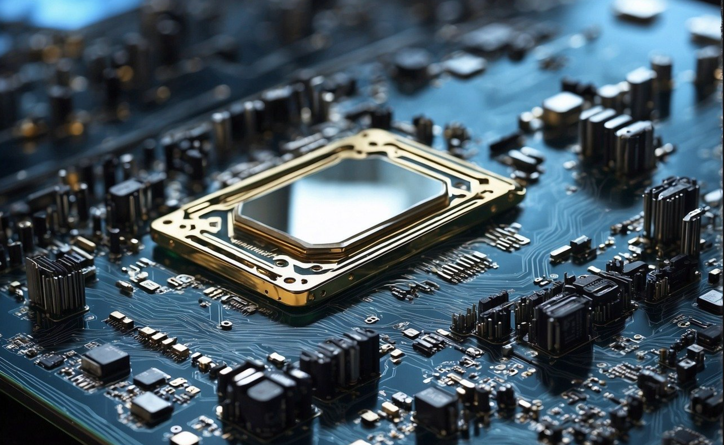
Scientists have developed a groundbreaking electric-field MRAM technology that offers ultra-low power use while preserving data without electricity. (CREDIT: CC BY-SA 4.0)
Memory technology has evolved quickly in recent years, driven by the need to improve on traditional systems. One promising candidate, Magnetoresistive Random Access Memory (MRAM), is gaining attention as a powerful alternative to standard volatile memory like DRAM.
MRAM stands out for its ability to retain data without power. It also offers greater durability and works well with CMOS chips. These qualities make it ideal for applications where both reliability and energy efficiency matter. Yet, one issue persists—how to cut down energy used during data writing.
A recent study in Advanced Science tackled this problem using a fresh approach. Instead of relying on the usual current-driven methods, the team explored electric-field-based techniques. This method could be key to solving MRAM’s power problem.
The research team from Osaka University introduced a new concept built on multiferroic heterostructures. These structures use layered materials that combine different electrical and magnetic properties. Their approach showed a major drop in energy needs during writing, pushing MRAM closer to low-power reality.
Electric-Field Switching and Power Consumption
Traditional MRAM works through magnetization switching using spin-transfer torque (STT) or spin-orbit torque (SOT). These methods pass electric currents through dense metals like platinum or tungsten. While fast and scalable, they waste a lot of energy through Joule heating—turning electricity into unwanted heat.
To avoid those losses, scientists began testing electric-field (E)-based switching. This method tweaks magnetization without the need for strong currents. Early work focused on semiconductors or thin ferromagnets on dielectric layers. But those designs often needed extra magnetic fields, which made them less useful in real-world, high-temperature settings.
Seeking better results, researchers turned to multiferroic materials. These combine ferromagnetic and piezoelectric layers. The layered structure responds well to electric fields and performs reliably at room temperature or higher. Best of all, it doesn’t need any outside magnetic field.
Related Stories
The Osaka team used a Heusler alloy, Co₂FeSi, paired with a piezoelectric called PMN-PT. They inserted a very thin layer of vanadium between the two. This tiny tweak helped grow a highly oriented (422) Co₂FeSi film—a key step for stronger electric control of magnetization.
Vanadium Insertion Enhances the Magnetoelectric Effect
That fine-tuning led to a massive leap in the so-called converse magnetoelectric (CME) effect. The CME effect happens when an electric field changes magnetization. In this study, the coupling coefficients topped 10⁻⁵ s/m—a notable milestone. By adjusting the thickness of the vanadium and Co₂FeSi layers, the team locked in stable magnetization control using just electric fields.
Lead author Takamasa Usami explained, “As MRAM devices rely on a non-volatile magnetization state rather than a volatile charge state in capacitors, they are a promising alternative to DRAM in terms of their low power consumption in the standby state.”
The use of PMN-PT substrates, which exhibit strong piezoelectric properties, was integral to the research. These materials enable efficient strain transfer between the piezoelectric and ferromagnetic layers, facilitating electric-field-induced changes in magnetization. This approach contrasts with earlier methods that relied on high-temperature treatments, often degrading piezoelectric performance.
One of the most striking achievements of this study was the realization of non-volatile binary states at zero electric field. By manipulating the sweeping operation of the electric field, the researchers demonstrated two distinct magnetization states that remained stable without additional energy input. This property addresses a key requirement for practical MRAM devices, where stable data storage at minimal power consumption is essential.
Magnetization Control at Room Temperature and Above
The stability of these states stems from the precise growth of the (422) Co2FeSi layer, facilitated by the vanadium insertion. X-ray diffraction measurements confirmed the absence of structural fluctuations, ensuring consistent magnetic properties across the device. This advancement contrasts with previous designs that suffered from in-plane structural inconsistencies, limiting their reliability.
Additionally, scanning transmission electron microscopy (STEM) analysis provided insights into the atomic structure of the heterostructure. These images revealed a clear and uniform interface between the Co2FeSi and PMN-PT layers, underscoring the effectiveness of the vanadium insertion in promoting epitaxial growth.
Senior author Kohei Hamaya noted, “Through precise control of the multiferroic heterostructures, two key requirements for implementing practical magnetoelectric MRAM devices are satisfied, namely a non-volatile binary state with zero electric field, and a giant CME effect.”
The implications of this research extend beyond energy-efficient memory storage. The demonstrated multiferroic heterostructure not only reduces power consumption but also enhances the scalability and reliability of MRAM. By eliminating the need for large currents, the technology mitigates heat generation and material degradation, paving the way for durable memory devices.
Scalable, Low-Power, and CMOS-Compatible
Moreover, the integration of multiferroic heterostructures into existing manufacturing processes is a significant advantage. The compatibility of these materials with CMOS technology ensures that they can be incorporated into a wide range of electronic devices without requiring extensive redesigns.
The ability to achieve robust performance at room temperature and above makes these devices suitable for a wide range of applications, from consumer electronics to industrial systems. For instance, wearable medical devices, which demand both low power consumption and reliable performance, could greatly benefit from this technology.
This breakthrough also highlights the potential for magnetoelectric MRAM (ME-MRAM) as a transformative technology in spintronics. The combination of electric-field-driven switching and non-volatility aligns with the demands of modern computing, offering a sustainable alternative to energy-intensive memory solutions.
Future developments could focus on further reducing the thickness of the ferromagnetic layers, enhancing speed, and minimizing power requirements even further.
Multiferroic MRAM Opens New Pathways for Spintronics
As the Osaka University team continues to refine their design, the future of MRAM looks increasingly promising. The integration of multiferroic heterostructures into practical devices could revolutionize memory storage, enabling energy-efficient, high-capacity systems that meet the needs of next-generation computing. Additionally, the principles demonstrated in this study could inspire new approaches to other spintronic applications, including logic devices and sensors.
The work also underscores the importance of interdisciplinary collaboration in advancing memory technologies. By combining expertise in materials science, physics, and engineering, researchers have created a pathway toward sustainable and scalable solutions for the growing demands of digital storage.
Note: Materials provided above by The Brighter Side of News. Content may be edited for style and length.
Like these kind of feel good stories? Get The Brighter Side of News' newsletter.