‘Magical’ ultra-thin lenses transform infrared light into visible light
New research shows how light can be bent, focused, and even changed in color using structures so small they’re invisible to the eye.
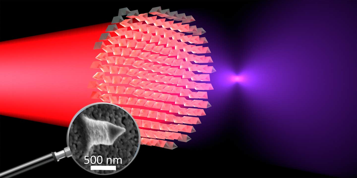
Infrared light passes through the metal lens and is converted into violet light and focussed in a focal point due to the material and the special surface structures – enlarged in the magnifying glass. (CREDIT: Ü.Talts / ETH Zurich)
In recent years, the world of optics has undergone a major shift. New research shows how light can be bent, focused, and even changed in color using structures so small they’re invisible to the eye. These structures, called metasurfaces, have unlocked powerful new abilities once thought impossible in lenses that are just nanometers thick.
Until now, building devices that use nonlinear optics—where one color of light transforms into another—has been costly and slow. But that’s changing fast thanks to the work of a team led by physicist Rachel Grange at ETH Zurich. By combining chemistry and nanotechnology, her group has developed a low-cost and scalable method to print ultra-thin lenses using a material called lithium niobate.
A new way to control light
Traditionally, optics relied on bulky lenses to bend light. Whether in a smartphone or a telescope, thick glass has long been essential for creating sharp images. But metalenses—a new class of ultra-thin lenses built from nanoscale structures—are now changing the rules.
Metalenses use nanostructures, often smaller than the wavelength of light, to steer, focus, or reshape light beams. These nanostructures, sometimes called “meta-atoms,” can change the phase and path of incoming light, performing many functions in one flat surface. When special materials are added to the mix, like lithium niobate, these metasurfaces become even more powerful, enabling nonlinear optical effects such as second-harmonic generation.
That’s when one color of light, such as infrared, passes through a nonlinear material and emerges as light with half the wavelength—like visible green light from a laser pointer. This behavior opens the door to many technologies, from compact spectrometers to new ways of imaging biological samples.
Challenges with lithium niobate
Lithium niobate is already a key material in the telecommunications industry because of its strong nonlinear properties. However, it’s notoriously hard to shape. Standard top-down techniques like etching often fail to produce the fine details needed for metasurfaces, especially at visible wavelengths. The harsh processes create slanted edges instead of vertical ones, reducing performance and control over light.
Related Stories
Moreover, monocrystalline lithium niobate has varying nonlinear tensor components that conflict with the symmetry needed in lens designs. This makes it tough to build uniform and high-performing optical devices using traditional fabrication methods.
To address these challenges, Grange’s team turned to a new approach called soft nanoimprinting.
Stamping light-manipulating structures
Instead of carving lithium niobate like stone, the ETH Zurich researchers developed a printable form of the material. They mixed liquid chemical precursors that form lithium niobate and stamped them into shape using molds made of soft silicon rubber.
“It works in a similar way to Gutenberg’s printing press,” said Ülle-Linda Talts, co-first author of the study and a doctoral student in Grange’s lab. Once heated to 600°C, the printed material crystallizes and forms a solid structure with strong nonlinear properties.
This technique allows for vertical nanostructures with aspect ratios as high as 6, which is key for focusing and steering light at short wavelengths.
The newly developed polycrystalline lithium niobate also retains a high nonlinear coefficient—around 4.8 picometers per volt at 880 nanometers—which is roughly 14% of the value for bulk single-crystal lithium niobate. That’s more than enough for powerful light conversion.
The process is fast, low-cost, and highly scalable. One mold can be used many times, making it suitable for mass production. It also avoids the steep costs and limitations of traditional nanofabrication, helping to bring advanced optics into a broader range of industries.
Shrinking spectroscopy tools
The researchers showed that their stamped lithium niobate metasurfaces can create metalenses that do more than just focus light. They can also change its color by doubling the frequency of incoming beams. For example, when an infrared laser with an 800-nanometer wavelength hits the metalens, visible light at 400 nanometers emerges, focused to a sharp point.
This effect, called second-harmonic generation, is one of the strongest forms of nonlinear optical behavior. It only happens in certain crystals without mirror symmetry or at surfaces of metallic materials like gold. But metals often lose power to heat, while crystalline materials like lithium niobate can handle much higher optical powers, making them ideal for practical uses.
Previous attempts to harness this effect in metasurfaces used materials like zinc oxide or gallium arsenide, but these had their own limitations—such as poor transparency in visible light or tricky crystal growth. Polycrystalline lithium niobate offers a more balanced and scalable solution.
Using their method, the ETH team achieved second-harmonic focusing over a wide spectral range—from near-ultraviolet to near-infrared wavelengths (760–1550 nanometers). They recorded up to 34 times greater nonlinear signal intensity, a big leap in performance.
A future for tiny optical tools
What makes these new lenses so exciting isn’t just their size or power—it’s what they could make possible. For instance, in the future, these devices could shrink down deep-UV light sources used in high-end chip manufacturing, making electronics fabrication faster and cheaper.
In other areas, the metalenses could be built into cameras or sensors to detect infrared light, which is usually invisible. That could help in everything from night vision systems to environmental sensors. Even more exciting is their potential in anti-counterfeiting. Because the nanostructures are too small to see or copy with standard tools, and because they produce nonlinear effects under specific light conditions, they could form the basis for secure banknotes, IDs, or artwork tags.
“You can’t see or feel the structures, but their optical fingerprint is unique,” Grange said. This makes them highly reliable for verifying authenticity in critical documents or valuable items.
And in research labs, these lenses could reduce the complexity of nonlinear microscopes. With the ability to focus and shift light frequencies on a single thin surface, scientists could design smaller, more mobile tools for studying cells or materials at very small scales.
A path to affordable nonlinear optics
Until recently, nonlinear optical devices required expensive crystals, delicate alignment, and complex equipment. The work from ETH Zurich offers a simpler path. Their soft nanoimprinting method uses common materials and allows for flexible design.
Because the molds can be reused and the printed material retains key nonlinear traits, this method could lead to the widespread use of nonlinear metasurfaces in consumer products, medical devices, and industrial tools.
While the field of metasurfaces is still young, researchers like Grange see it growing fast. “We have only scratched the surface so far and are very excited to see how much of an impact this type of new cost-effective technology will have in the future,” she said.
Her team's results show that precision optics doesn’t have to be bulky, expensive, or fragile. With clever design and new fabrication tools, the future of light manipulation is both ultra-thin and highly capable.
Research findings are available online in the journal Advanced Materials.
Note: The article above provided above by The Brighter Side of News.
Like these kind of feel good stories? Get The Brighter Side of News' newsletter.