Scientists Create World’s First Semiconductor Made From Graphene
These semiconductors, pivotal components of electronic devices, represent a monumental leap forward in the realm of technology.
Researchers have ushered in a new era of electronics by crafting the world's inaugural functional semiconductor from graphene. (CREDIT: Chris McKenney)
Researchers at the Georgia Institute of Technology have ushered in a new era of electronics by crafting the world's inaugural functional semiconductor from graphene, an extraordinary material composed of a single layer of carbon atoms bonded together with unmatched strength.
These semiconductors, pivotal components of electronic devices, represent a monumental leap forward in the realm of technology.
At a time when the predominant material for electronic devices, silicon, is grappling with its limitations amidst the escalating demands for faster computing and diminutive gadgets, this achievement marks a significant breakthrough.
Spearheaded by Walter de Heer, a distinguished Regents' Professor of physics at Georgia Tech, the team embarked on a journey that culminated in the creation of a graphene semiconductor seamlessly compatible with traditional microelectronics processing methods—a prerequisite for any viable substitute to silicon.
Related Stories
The crux of their triumph lies in surmounting a longstanding obstacle that has long thwarted graphene research: the absence of a crucial electronic property known as the "band gap."
This elusive attribute is indispensable for semiconductors to toggle between states of conductivity and non-conductivity, a fundamental function in electronic devices. Graphene, until now, had been bereft of this essential feature.
"We now have an extremely robust graphene semiconductor with 10 times the mobility of silicon, and which also has unique properties not available in silicon," de Heer remarked, underlining the significance of their accomplishment. "But the story of our work for the past 10 years has been, 'Can we get this material to be good enough to work?'"
Zhao, J. et al. Ultrahigh-mobility semiconducting epitaxial graphene on silicon carbide. (CREDIT: Nature)
De Heer's foray into exploring carbon-based materials as potential semiconductors dates back to the nascent stages of his career, with his transition to investigating 2D graphene materializing in 2001. Motivated by the tantalizing prospect of integrating graphene's exceptional properties into electronics, de Heer envisioned a path towards innovation.
"We were motivated by the hope of introducing three special properties of graphene into electronics," he explained. "It's an extremely robust material, one that can handle very large currents, and can do so without heating up and falling apart."
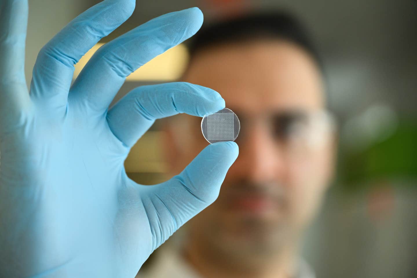
Researchers produced epitaxial graphene, which is a single layer that grows on a crystal face of the silicon carbide. (CREDIT: Chris McKenney)
The pivotal breakthrough came with the realization of growing graphene on silicon carbide wafers using specialized furnaces, resulting in epitaxial graphene—a single-layered structure intricately bonded to the crystal face of silicon carbide. Through meticulous refinement efforts spanning a decade, the team, in collaboration with colleagues at Tianjin University in China, honed the material to perfection, laying the groundwork for its transformative potential.
In its natural state, graphene assumes the guise of a semimetal, neither wholly semiconductor nor metal. The pivotal challenge lay in imbuing graphene with the capability to emulate silicon's functionality, necessitating precise manipulation without compromising its inherent properties. The introduction of doping—an atom-based technique to donate electrons to the system—proved instrumental in gauging the material's conduciveness without causing damage.
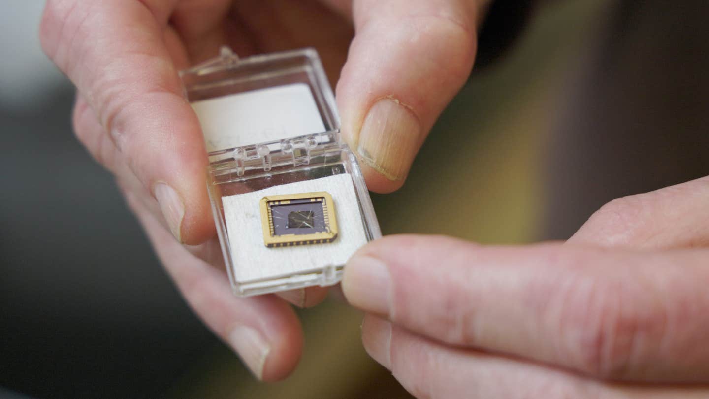
The team's meticulous measurements revealed that their graphene semiconductor boasted a remarkable tenfold increase in mobility compared to silicon. (CREDIT: Chris McKenney)
The team's meticulous measurements revealed that their graphene semiconductor boasted a remarkable tenfold increase in mobility compared to silicon, signifying enhanced electron movement with minimal resistance—an attribute conducive to expedited computing processes.
"A long-standing problem in graphene electronics is that graphene didn’t have the right band gap and couldn’t switch on and off at the correct ratio,” Lei Ma elucidated. “Over the years, many have tried to address this with a variety of methods. Our technology achieves the band gap, and is a crucial step in realizing graphene-based electronics."
The advent of epitaxial graphene heralds a paradigm shift in electronics. (CREDIT: Chris McKenney)
The advent of epitaxial graphene heralds a paradigm shift in electronics, presenting a fertile landscape for pioneering technologies harnessing its unique properties. Notably, the material's capacity to leverage the quantum mechanical wave properties of electrons holds profound implications for quantum computing—a tantalizing prospect on the horizon.
"Our motivation for doing graphene electronics has been there for a long time, and the rest was just making it happen," de Heer reflected. "We had to learn how to treat the material, how to make it better and better, and finally how to measure the properties. That took a very, very long time."
Looking ahead, de Heer envisions a trajectory akin to the evolution of electronics, with graphene poised to assume the mantle from silicon—a transition mirroring the progression from vacuum tubes to silicon-based devices.
Just as the Wright brothers' pioneering flight transformed the realm of transportation, epitaxial graphene holds the promise of reshaping the landscape of electronics, propelling innovation to uncharted territories.
Note: Materials provided above by The Brighter Side of News. Content may be edited for style and length.
Like these kind of feel good stories? Get the Brighter Side of News' newsletter.