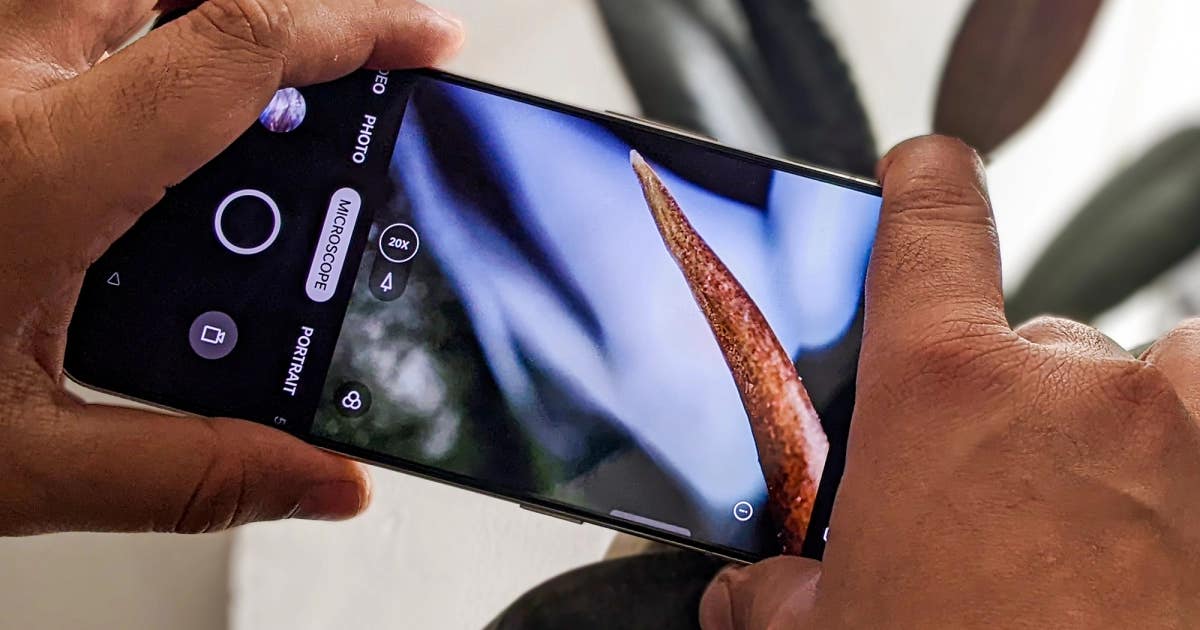
SMART technology converts existing mobile phone cameras into high-resolution microscopes
The world’s smallest LED, smaller than the wavelength of light, can transform mobile phone cameras into high-resolution microscopes.
[May 5, 2023: Staff Writer, The Brighter Side of News]
The world's smallest LED, smaller than the wavelength of light, can transform mobile phone cameras into high-resolution microscopes.. (CREDIT: Creative Commons)
In a world where technological innovation continues to reshape our lives, a groundbreaking development has been achieved in the realm of photonics and micro-imaging.
Researchers from the Singapore-MIT Alliance for Research and Technology (SMART), specifically from the Disruptive & Sustainable Technologies for Agricultural Precision (DiSTAP) and the Critical Analytics for Manufacturing Personalized-Medicine (CAMP) Interdisciplinary Research Groups (IRGs), have created the world's smallest LED, smaller than the wavelength of light, that can transform mobile phone cameras into high-resolution microscopes.
This pioneering advancement revolutionises the way we perceive everyday devices, offering a significant leap forward in the miniaturisation of diagnostics. This has promising implications for indoor farmers and sustainable agriculture, enabling detailed analysis without the need for bulky conventional microscopes.
The results of the research were published in two separate papers. The first, titled "A sub-wavelength Si LED integrated in a CMOS platform" was featured in Nature Communications. The second, "Simultaneous spectral recovery and CMOS micro-LED holography with an untrained deep neural network" was published in the journal Optica.
Related Stories
Transforming Mobile Phone Cameras into Microscopes
The first breakthrough involved the development of a tiny LED light, smaller than the wavelength of light itself. This innovative LED was used to build the smallest holographic microscope in the world, a development that could see everyday devices such as mobile phones converted into microscopes through modifications to the silicon chip and software.
The LED developed by SMART researchers is a CMOS-integrated sub-wavelength scale LED, exhibiting high spatial intensity and the smallest emission area among all known silicon emitters in scientific literature. The researchers integrated this LED into a compact, all-silicon holographic microscope requiring no lens or pinhole, a significant step forward in the field known as lensless holography.
Revolutionising Image Reconstruction with Neural Networking Algorithm
The second breakthrough involves a revolutionary neural networking algorithm that reconstructs objects measured by the holographic microscope, further enhancing the examination of microscopic objects like cells and bacteria. Traditional reconstruction methods require detailed knowledge of the experimental setup and are sensitive to difficult-to-control variables such as optical aberrations, the presence of noise, and the twin image problem.
Device structure and emission spectra. Photograph of a fully fabricated 300 mm wafer with monolithic electronics and photonics, and optical micrograph of a diced, unpackaged chip with different active and passive photonic components and mixed-signal circuits integrated side-by-side, and close-ups of the LED and the reference emitter on this chip. (CREDIT: Nature Communications)
SMART researchers developed a deep neural network architecture that improves the quality of image reconstruction. This innovative neural network, which requires no training data, is designed to increase contrast and take into account the wide spectral bandwidth of the source. It offers blind source spectrum recovery from a single diffracted intensity pattern, marking a significant departure from traditional supervised learning techniques.
Promising Future Applications
The combination of CMOS micro-LEDs and the neural network paves the way for other computational imaging applications such as compact microscopes for live-cell tracking or spectroscopic imaging of biological tissues like living plants. Already, in-line holography microscopes have been used for various applications, including environmental monitoring and biological sample imaging. The researchers are optimistic that this work could also lead to the next generation of on-chip imaging systems.
Illustration of the process of image reconstruction using the LED holographic microscope and neural network. (CREDIT: Singapore-MIT Alliance for Research and Technology (SMART))
Iksung Kang, lead author of the Optica paper and Research Assistant at MIT at the time of this research, explained, “Our breakthrough represents a proof of concept that could be hugely impactful for numerous applications requiring the use of micro-LEDs. For instance, this LED could be combined into an array for higher levels of illumination needed for larger-scale applications. Furthermore, control electronics and even the imager could be integrated into the same chip by exploiting the available electronics in the process, thus creating an ‘all-in-one’ micro-LED that could be transformative for the field.”
Rajeev Ram, Principal Investigator at SMART CAMP and DiSTAP and Professor of Electrical Engineering at MIT, further expounded on the potential applications of the novel LED. “Our new LED has immense potential not only in lensless holography but also in a wide range of other applications.
Given that its wavelength is within the minimum absorption window of biological tissues and its high intensity and nanoscale emission area, our LED could be ideal for bio-imaging and bio-sensing applications. This includes near-field microscopy and implantable CMOS devices," he said.
Ram also highlighted the potential for the LED to be integrated with on-chip photodetectors, opening up possibilities for on-chip communication, NIR proximity sensing, and on-wafer testing of photonics. "The possibilities are immense, and we are only scratching the surface of what this technology can achieve," he added.
The creation of this new LED and the corresponding neural network represents a significant stride in the field of photonics, overcoming long-standing challenges in the creation of a powerful on-chip emitter smaller than a micrometre.
Currently, the light in most photonic chips originates from off-chip sources, leading to lower overall energy efficiency and limitations in the scalability of these chips. The research team's development of an on-chip emitter using silicon – a material that has shown potential but has been limited by low quantum efficiency due to the indirect bandgap – addresses these issues head-on.
This research was made possible through the support of the National Research Foundation (NRF) Singapore under its Campus for Research Excellence and Technological Enterprise (CREATE) programme. The programme seeks to foster research innovation and technological advancement, with this groundbreaking research standing as a testament to its success.
Digital in-line holography setup and results. Schematic of the experimental setup demonstrating in-line holographic imaging of 20 μm diameter latex beads with a single LED (bias current at 6.5 mA) as the illumination source. Close-up on the left illustrates the interference pattern formed between the incident light and the scattered light from a bead. (CREDIT: Nature Communications)
In the long term, this development could revolutionise several industries and sectors, including agriculture, medicine, environmental monitoring, and more. By making microscopic examination accessible through everyday devices like mobile phones, this technology could democratise access to high-resolution imaging, a boon for researchers, educators, and the general public alike.
The researchers are optimistic that the adoption and adaptation of this technology will spur more innovation and improvements. "The possibilities are vast," Kang said. "It's an exciting time to be working in photonics and microimaging. We're excited to see where this technology will take us in the years to come." With this breakthrough, we inch closer to a future where the line between our everyday gadgets and high-tech scientific equipment becomes increasingly blurred.
For more science and technology news stories check out our New Innovations section at The Brighter Side of News.
Note: Materials provided above by The Brighter Side of News. Content may be edited for style and length.
Like these kind of feel good stories? Get the Brighter Side of News' newsletter.