Thin, new design doubles the efficiency of OLED lights
KAIST reports a near-planar outcoupling design that more than doubles OLED light efficiency while keeping screens flat.

 Edited By: Joseph Shavit
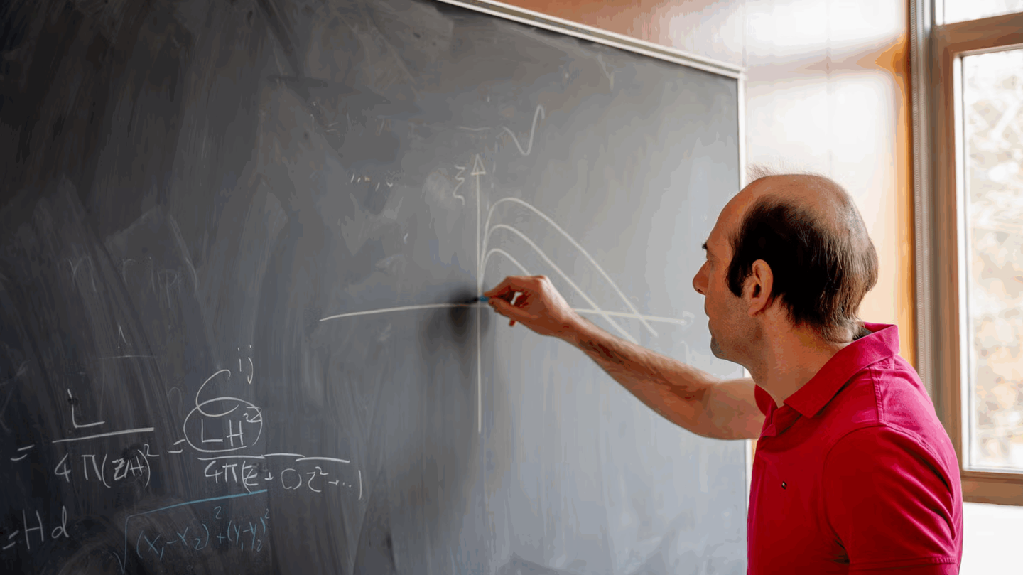
A new KAIST design targets trapped OLED light at the pixel level, boosting efficiency over twofold without sacrificing a flat display. (CREDIT: Shutterstock)
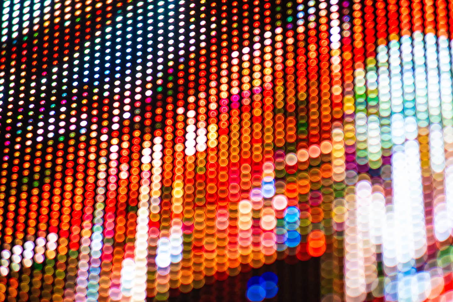
OLED screens already feel like magic. Colors pop on your phone. Blacks look truly black on your TV. The panel stays thin, smooth, and flexible. Yet a stubborn problem inside the device keeps engineers from pushing brightness much further without paying a price in power and heat.
Researchers at KAIST say they have found a way around that limit. On Jan. 11, the institute announced a new near-planar light outcoupling structure and an OLED design method that can cut internal light loss. The team, led by Professor Seunghyup Yoo of the School of Electrical Engineering, reports that the combined approach can more than double light-emission efficiency in small pixels while keeping OLED’s flat form.
The idea targets a hidden waste. OLEDs create light inside stacked, ultrathin organic layers. As that light tries to leave, it reflects and gets absorbed again and again. KAIST says more than 80% of the light can vanish as heat before it ever escapes.
The Light You Never Get to See
That trapped light matters because it forces a trade-off you feel every day. If you want a brighter screen, the device often needs more power. More power can mean more heat. On a phone or tablet, that can also affect battery life.
Engineers have tried to rescue that wasted light with add-on structures. A hemispherical lens can extract lots of light. But it also sticks out. That bulge fights the thin, flat look that makes OLEDs so appealing.
Microlens arrays, often called MLAs, avoid a big bump. They can be made thin and spread across a surface. Yet they come with their own problem. They usually need a larger area than a single pixel to work well. In a display packed with tiny pixels, that can cause interference between neighboring pixels.
KAIST says its new approach aims to get strong light extraction inside each pixel’s own footprint. That pixel-level focus matters because displays are not one giant light source. They are millions of small ones, each expected to stay sharp and separate.
A Design Built for Real Pixels
Many older OLED designs start with a simplifying assumption. They treat the OLED as if it extends infinitely. That makes the math easier. It also ignores the real geometry of a working display.
The KAIST team built a strategy that respects the finite size of actual pixels. By designing around the true pixel boundaries, the researchers say they can send more light outward from pixels of the same size.
The team also built a new near-planar outcoupling structure. It stays thin, about as thin as existing MLAs. It also keeps the OLED surface almost flat, which helps preserve a key OLED advantage.
KAIST says the structure guides light out efficiently in the forward direction. It also avoids spreading that light too widely. That matters for perceived brightness because viewers typically look straight at the screen.
In a simple sense, the design tries to do two things at once. It helps trapped light find an exit. It also helps that light exit in a useful direction.
A Thin Structure With a Big Payoff
KAIST says the near-planar structure achieves light extraction close to a hemispherical lens of the same lateral dimension. That is a meaningful claim because hemispherical lenses set a high bar for extraction. They also create a form-factor problem.
By keeping the structure thin, the approach “hardly undermines the flat form factors of OLEDs,” according to the announcement. That makes it easier to apply to flexible OLED displays, where bumps and thickness can cause mechanical issues.
The researchers report that when they combined the new OLED design method with the near-planar structure, they achieved more than a twofold improvement in light-emission efficiency, even in small pixels. That detail matters for real products. Small pixels define high-resolution screens.
The work also speaks to the daily experience of using OLED devices. Higher light-emission efficiency means you can get the same brightness with less power. It also means you can push brightness without the same heat load.
That shift could change how designers balance features in future phones and tablets. A screen can remain vivid without draining the battery as quickly.
Voices From the Lab
The team frames the advance as both practical and personal. MinJae Kim, the first author of the study, said, “A small idea that came up during class was developed into real research results through the KAIST Undergraduate Research Program (URP).”
Yoo also emphasized why pixel size matters for display use. “Although many light outcoupling structures have been proposed, most were designed for large-area lighting applications, and many were difficult to apply effectively to displays composed of numerous small pixels,” he said.
He described the goal as reducing pixel-to-pixel interference while pushing efficiency upward. “The near-planar light outcoupling structure proposed in this work was designed with constraints on the size of the light source within each pixel, reducing optical interference between adjacent pixels while maximizing efficiency,” Yoo said.
He also said the method reaches beyond OLEDs. He noted it can apply to next-generation displays based on materials such as perovskites and quantum dots.
Practical Implications of the Research
If this approach scales, it could make brighter displays possible without raising power use. That can extend battery life in smartphones and tablets. It can also reduce heat generation, which helps devices feel more comfortable in your hand.
Higher efficiency can also support longer display lifespan. Lower heat and lower electrical stress can ease wear over time. For consumers, that can mean screens that stay strong longer.
For research and industry, the work pushes light extraction into the pixel era. It treats a display as millions of finite sources, not one infinite sheet. That shift can guide new optical designs for dense, high-resolution panels. It may also carry over to emerging display materials, including perovskites and quantum dots, as Yoo noted.
Over time, better light extraction can cut energy demand across billions of screens, which benefits both costs and sustainability.
Research findings are available online in the journal Nature Communications.
The original story "Thin, new design doubles the efficiency of OLED lights" is published in The Brighter Side of News.
Related Stories
- New discovery substantially increases the brightness of OLED displays
- New 3D-printable material paves the way for cheaper and sustainable OLED televisions and smartphones
- Scientists create first-ever stretchable quantum dot television display
Like these kind of feel good stories? Get The Brighter Side of News' newsletter.
Joshua Shavit
Writer and Editor
Joshua Shavit is a NorCal-based science and technology writer with a passion for exploring the breakthroughs shaping the future. As a co-founder of The Brighter Side of News, he focuses on positive and transformative advancements in technology, physics, engineering, robotics, and astronomy. Joshua's work highlights the innovators behind the ideas, bringing readers closer to the people driving progress.