New atomic-layer memory keeps 100% of its data intact after 23 months in space
A tiny memory array kept the letters FDU intact through 23 months in orbit. Combined with high-dose radiation tests on Earth, the result offers a practical step toward more reliable space electronics.

 Editor: Joseph Shavit

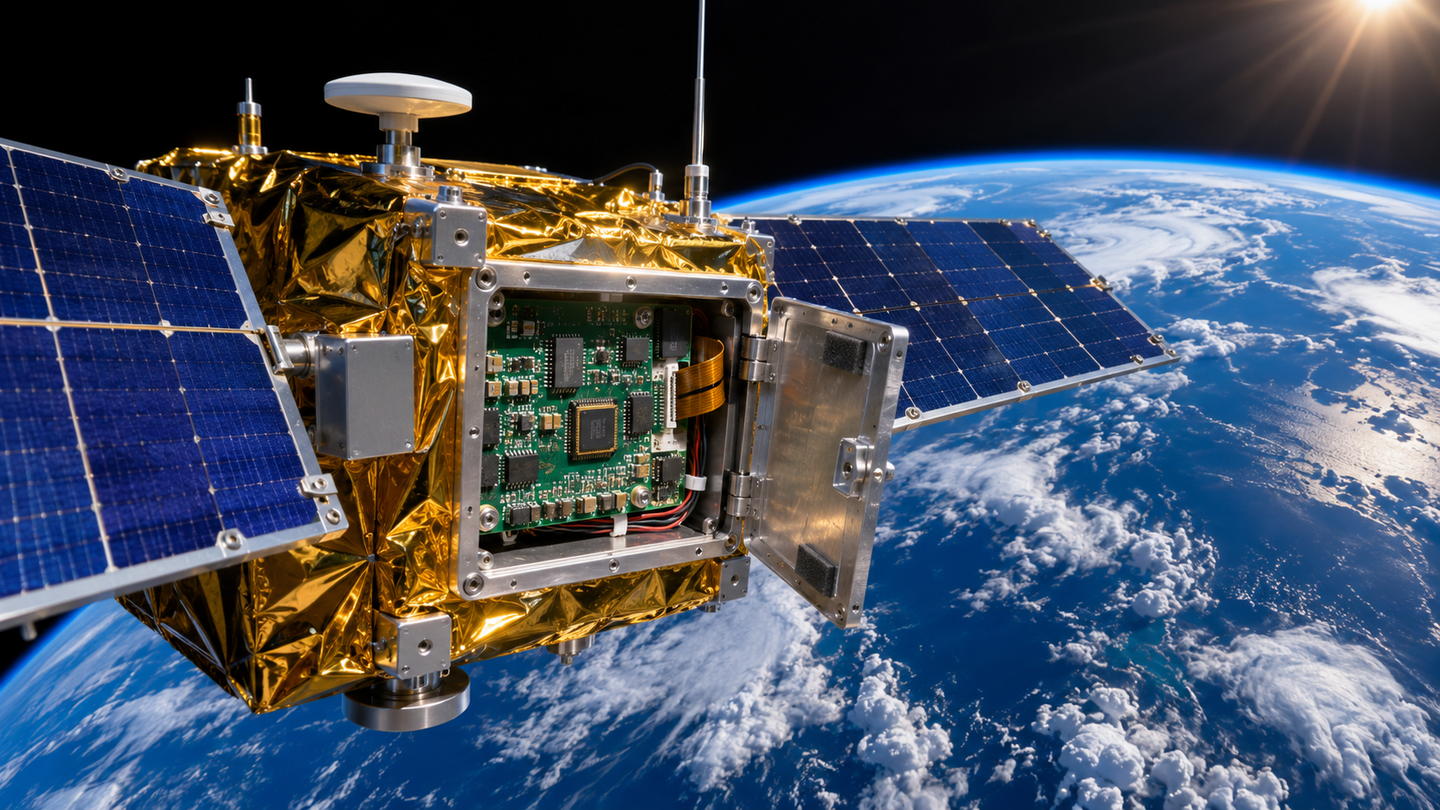
Artist’s visualization of satellite electronics above Earth. A Fudan University atomic-layer memory array retained its programmed data during 23 months in orbit, with all reported complete readouts matching the original message. (CREDIT: The Brighter Side of News)
For nearly two years, a small memory array circling Earth has held onto a very short message: FDU. Those three letters might seem modest beside the images and measurements satellites routinely collect, but keeping them intact was the point. The experiment asked whether an atomically thin semiconductor could preserve information while operating in space.
Researchers at Fudan University report that, after 23 months in orbit, the returned memory data remained 100% accurate. Their study, published in National Science Review, combines that flight demonstration with radiation tests on Earth. Peng Zhou, the corresponding author, led the work.
The challenge is familiar to anyone designing spacecraft electronics. A satellite depends on stored instructions and scientific data, yet radiation can change the electrical behavior of the devices holding them. As ambitions for orbital computing grow, reliable storage becomes an increasingly important part of making those systems work.
A tiny message puts atomic-layer memory to the test
The array traveled aboard the Fudan No.1 Lancang-Mekong Future Satellite, launched September 24, 2024. It entered a sun-synchronous low Earth orbit about 517 kilometers above the surface. From there, the satellite could read the memory and send its contents to a ground station, letting researchers check performance during the mission.
To store FDU, the team encoded each letter using five binary bits, the zeros and ones that electronic memory represents through distinguishable electrical states. Three letters therefore required 15 bits. Each five-bit memory cell used five transistors, and the demonstration array occupied a die measuring one centimeter on each side.
All reported complete readout records matched the programmed message, without error-correction codes, majority voting or extra redundancy. That gives the result a clear, limited meaning: the stored test pattern remained readable in the returned records. It is a small demonstration of retention, alongside broader efforts to improve memory devices.
The team describes this as the first real-time, on-orbit test of atomic-layer memory. Checking a device while it operates adds evidence that laboratory irradiation and measurements after a flight cannot provide alone. Much like testing satellite communications, it brings the hardware into the environment where it must eventually do its job.
Why making the active layer thinner could help
The memory uses molybdenum disulfide, usually shortened to MoS2, as its semiconductor. Its active channel consists of a monolayer, an extraordinarily thin layer through which electrical charge moves. The researchers fabricated their devices using a process built around a two-inch wafer, connecting the material’s unusual properties with a route toward making arrays.
Radiation can create defects and places where charge becomes trapped. Those changes can shift a transistor’s current or disturb the distinction between stored states. Research on energetic particles helps explain why space poses such a demanding test for electronics, even when the hardware stays relatively close to Earth.
An atomically thin channel offers less material in which certain radiation-induced defects can accumulate. The device’s interfaces and arrangement also matter, however. Here, the researchers used a back-gate design that helps protect the insulating layer and reduce radiation damage, combining material choice with the physical layout of the transistor.
That combination matters because the goal goes beyond producing an exceptionally thin component. The component must keep behaving predictably after exposure. Other approaches pursue heat-resistant memory, while this work concentrates on radiation tolerance and readable electrical signals.
Ground tests keep zeros and ones far apart
The flight experiment shows what happened along one satellite’s journey. To investigate how the devices handled a much larger accumulated radiation dose, the team also exposed them to cobalt-60 gamma rays on Earth. The tests reached 20 Mrad, equivalent to 20 million rad of absorbed radiation dose.
After irradiation, the transistors maintained stable ratios between their on and off currents. In the memory devices, the read currents representing zero and one differed by approximately eight orders of magnitude, or a factor of 100 million. That large separation gives the reader considerable room to tell one state from the other.
The distinction is central to electronic memory. A stored state becomes less useful if its electrical signature drifts toward the other state. These measurements show that the two remained clearly distinguishable under the reported exposure, giving researchers another way to assess the encouraging orbital result.
Ground irradiation and space operation therefore answer related questions from different directions. One subjects devices to a controlled dose, while the other follows actual performance in orbit. Together, they help connect laboratory development with the practical demands facing space missions.
A quiet electrical signal makes reading easier
Keeping the two states far apart solves only part of the readout problem. Their currents must also remain sufficiently steady. Electrical noise consists of unwanted fluctuations, and if those fluctuations grow, a reading can become harder to interpret even when the underlying memory state has survived.
The researchers paid particular attention to low-frequency noise, which can increase when radiation creates additional traps and defects. Their atomic-layer devices retained their low-noise characteristics after the 20 Mrad exposure. That stability supported data readout at picoampere current levels, where even small unwanted fluctuations deserve attention.
A picoampere is one-trillionth of an ampere. Reading reliably with such small currents could help reduce the electrical demands of future devices, an aim shared with work on efficient hardware. The result concerns the memory’s measured behavior, with further integration still needed to establish the performance of a complete system.
The paper also notes room for improvement in fabrication, including cleaner surfaces and better interfaces. Radiation resilience and manufacturing quality both influence the final signal. That makes low-noise operation part of the engineering work, alongside the wider search for dependable storage technologies.
What the 500-year estimate actually describes
The researchers estimate that accumulating a dose equivalent to 20 Mrad could take up to 500 years in their target radiation environment. Their calculation assumes a sun-synchronous orbit at 550 kilometers and shielding equivalent to at least 0.25 millimeters of aluminum. It translates a tested dose into time under those assumptions.
That estimate extends far beyond the 23 months actually observed in flight. It addresses one aspect of durability, since a component’s full working life also depends on the other conditions it encounters. The orbital demonstration establishes retention over the reported mission interval, while the ground tests help explore its radiation margin.
The devices are nonvolatile and one-time programmable, characteristics the authors see as suitable for firmware and other information intended to remain fixed. Nonvolatile memory retains its information when power is removed, an important property for stored instructions that a satellite may need when its electronics start up again. Wider use will depend on incorporating the memory into working systems, much as other integrated chips must connect a device-level idea with practical circuitry.
For now, three unchanged letters provide a tangible starting point. The team has shown that this small array can store information in orbit and return readable results, strengthening the case for further development of atomic-scale electronics.
Dig deeper into memory and electronics for space
These studies explore related approaches to reliable storage, atomic-layer devices and testing beyond the laboratory.
- Georgia Tech Researchers Discover New Form of NAND Flash Data Storage for Deep Space Missions: Describes a ferroelectric approach to radiation-resilient storage that encodes data through polarization rather than trapped charge. (Georgia Institute of Technology, May 2026)
- Radiation-tolerant atomic-layer-scale RF system for spaceborne communication: Reports a MoS2-based radio-frequency system and evaluates its communication performance during nine months of orbital operation. (Nature, January 2026)
- Quasi-non-volatile capacitorless DRAM based on ultralow-leakage edge-contact MoS2 transistors: Explores how transistor contacts and very low leakage currents can improve memory retention in a different MoS2-based device architecture. (Nature Materials, January 2026)
- Space environment adaptability of 2D semiconductor materials: Examines two-dimensional semiconductor materials and devices following a 14-day spaceflight, providing context for evaluating how space exposure changes their properties. (National Science Review, February 2025)
- A scalable integration process for ultrafast two-dimensional flash memory: Investigates a manufacturing approach for integrating two-dimensional flash-memory devices into arrays, addressing the gap between individual components and larger circuits. (Nature Electronics, August 2024)
Research findings are available online in the journal National Science Review.
The original story "New atomic-layer memory keeps 100% of its data intact after 23 months in space" is published in The Brighter Side of News.
Related Stories
- Breakthrough MRAM chips deliver faster, ultra-efficient computer memory
- Scientists reshape light to control magnetic memory and a material's magnetic properties
- New material stores four magnetic states per cell - exponentially increasing memory storage
Like these kind of feel good stories? Get The Brighter Side of News' newsletter.
Joshua Shavit
Writer and Editor
Joshua Shavit is a NorCal-based science and technology writer with a passion for exploring the breakthroughs shaping the future. As a co-founder of The Brighter Side of News, he focuses on positive and transformative advancements in technology, physics, engineering, robotics, and astronomy. Having published articles on AOL.com, MSN, Yahoo News, and Ground News, Joshua's work highlights the innovators behind the ideas, bringing readers closer to the people driving progress.